

Circuiti stampati professionali, multistrato e speciali
Printed circuit boards - multilayers and specials PCB
A little history of the printed circuit...
The PCBS from the 1950s to today
Now in Italy, the printed circuit board (also called PCBS, acronym for printed circuit board) has more than half a century of history behind it, given that its history in Italy began towards the end of the 50’s: in fact, dating back to this period the first monorame printed circuits creations were produced for electro-mechanical field applications.
In those days laminates for printed circuits in bakelite were used (which subsequently took the name of 3XPC). The drawings of the tracks on these circuits were printed with the serigraphy method, and the etching of the copper was carried out by using cupric chloride, ferric chloride or sulfo-cromiche mixtures; the holes were formed by punching, together with the contour, while the protection of the tracks (in order to avoid oxidation) was carried out with an aqueous or alcohol solution of Greek pitch (rosin) which also had an excellent flux power during the sublimation welding phase.
During the early sixties the production of the first double face printed circuits, characterized by metallized through holes (Plated Through Hole); began in Italy these printed circuits were made on laminated glass fibre impregnated in epoxy resin called G10, or more commonly vetronite (the current FR4); these PCBS were also called professional printed circuits, to differentiate them from single sided/monofaccia printed circuits which were instead classified as civilian printed circuits.
The circuits with metallized holes were always made with silk-screen printing but in negative, and only after the mid 1960s the use of liquid photoresist began, which after brief period was replaced with dry film. The metallization process of the holes was for chemical deposition of dissolved copper in Signette salts of (a technology known for centuries, because this is the same that allowed to deposit palladium and copper on glass to make mirrors); the holes so metallized were subsequently reinforced with with a galvanic process in a solution of copper sulphate. The tracks were at this point covered with pure tin (tin Culmo, which appeared glossy) or tin/lead (which appeared opaque and poor for welding); such coatings also had the function of etch resistance, i.e. resistance of incision, and resisted to baths of sulfuric acid and hydrogen peroxide, ammonium persulfate or cupro ammoniacal nitrogen solution that was needed to remove the unprotected copper, leaving only the tracks and the metallized holes. In the case of circuits produced with tin/lead, (SnPb 63/37) a thermal process was necessary, it was called remelting or suffusion which made the surface perfectly weldable: these treatments were initially carried out by immersing the printed circuits in a bath of boiling oil at 240°C.
In Italy, towards the middle of the seventies the first furnaces for recasting infrared appeared, very similar to the furnaces used for welding of the SMD components. The need to limit the areas of bonding of the printed circuit board was born toward the end of the sixties using precisely the solder resist printed in silk-screen printing, which was normally green. In the same period, in the United States the first productions of multilayer printed circuits began, i.e. with copper tracks also between the layers of glass fibre inside the laminate. In this way the metallized holes intercepted the copper pads of the internal layers and therefore increased the number of possible connections. This technique is the one that has allowed us to begin producing increasingly complex printed circuits and with a component density always closer to 100% of the available surface.
Baselectron Printed Circuits
Go to product data sheets
The solution for lighting and automotive sectors; high quality, low heat.
Flex-pcb with aluminum heatsink
Note:
The printed circuits are also called differently depending on their characteristics, for example:

Single sided
Monolayer and Single side are different ways to identify a printed circuit with a single side or with a single layer of tracks.
Double sided
Double side and bilayer there are different ways to identify a printed circuit with dual sides or with the tracks on both surfaces.
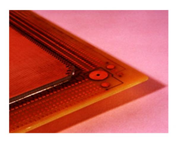
Multilayer
Multilayer MLB are the names that are used to identify multilayer printed circuits with additional layers of internal tracks.
Solder
Solder resist or solder mask is what is called the usually green protective layer that limits the welding to only the pads and also leaves the comb connectors and mechanical contacts uncovered, it is often shortened to solder.